2D FDM-based PCB thermal simulator, built in pure Python.
Generates a thermal camera-style temperature heatmap from the board's 3D model (STEP) and a component thermal parameter table (CSV).
Designed for preliminary thermal analysis of electronic designs without the need for industrial FEM tools.


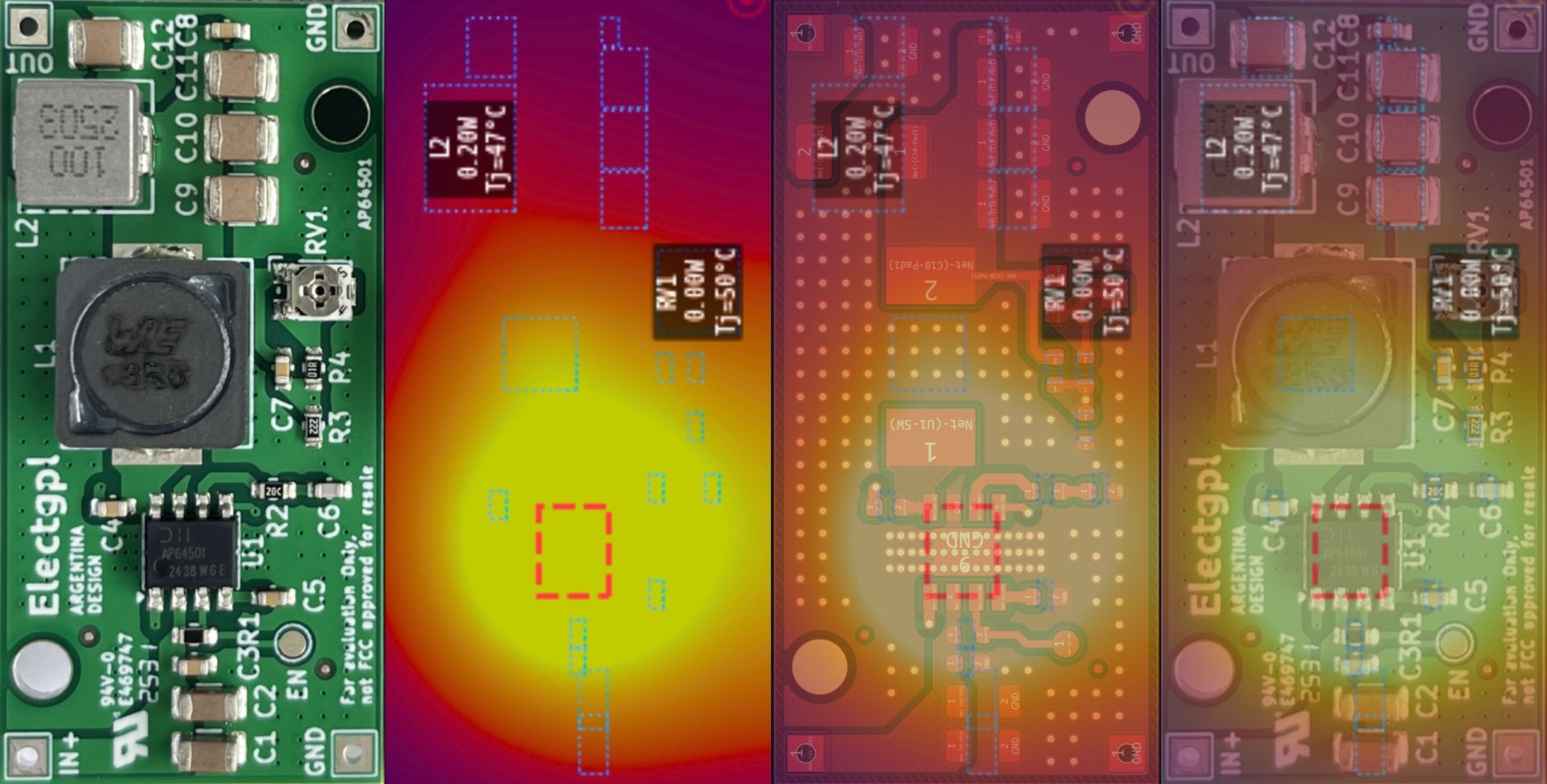

The system generates three output files:
| File | Contents |
|---|---|
pcb_thermal_map.png |
Heatmap overlaid on the board, 300 DPI |
tj_analysis.png |
Junction temperature table per component |
pcb_thermal_map_Tmatrix.npy |
NumPy temperature matrix for post-processing |
The simulator solves the 2D steady-state heat conduction equation:
∇·(k_eff ∇T) - (2h/t)·(T - T_amb) + q = 0
where:
| Symbol | Meaning | Unit |
|---|---|---|
k_eff |
Effective thermal conductivity of the stack-up | W/m·K |
h |
Surface convection coefficient | W/m²·K |
t |
PCB thickness | m |
T_amb |
Ambient temperature | °C |
q |
Dissipated power density | W/m³ |
The 2h/t term models convection on both PCB faces (top and bottom) as a volumetric heat sink. This is valid when the Biot number Bi = h·t/(2·k_eff) << 0.1 — a condition that is verified automatically at startup.
A PCB is an anisotropic composite material. The model computes k_eff separately for each direction:
In-plane (X,Y) — layers in thermal parallel:
k_eff_xy = (k_Cu × t_Cu + k_FR4 × t_FR4) / t_total
Through-plane (Z) — layers in thermal series:
k_eff_z = t_total / (t_Cu/k_Cu + t_FR4/k_FR4)
For typical values of 2 layers at 1 oz (35 µm, fill factor 0.35) on 1.6 mm FR4:
k_eff_xy ≈ 6.2 W/m·K(copper dominates in parallel)k_eff_z ≈ 0.30 W/m·K(FR4 dominates in series)
The equation is discretized on a regular grid using centered finite differences. For each interior node (i,j):
k/dx² × (T[i+1,j] + T[i-1,j] - 2T[i,j])
+ k/dy² × (T[i,j+1] + T[i,j-1] - 2T[i,j])
- (2h/t) × (T[i,j] - T_amb)
+ q[i,j]/t = 0
This produces a linear system A·T = b where A is a sparse symmetric positive-definite matrix. The system is solved with scipy.sparse.linalg.spsolve (SuperLU). For a 400×200 = 80,000-node grid, solve time is under 1 second.
Boundary conditions on all four PCB edges are homogeneous Neumann (∂T/∂n = 0), assuming no heat flows through the board edges.
The junction temperature of each component is estimated as:
T_j = T_PCB_surface + P × θ_JC
where T_PCB_surface is the FDM-computed temperature directly beneath the component's footprint. This is more accurate than the standard JEDEC point model (T_amb + P × θ_JA) because it accounts for the thermal influence of neighboring components on the board surface.
pcb_thermal_sim/
│
├── main.py                # Main pipeline. Entry point.
├── config.py              # PCB and simulation parameters
├── material_properties.py # Stack-up effective conductivity
├── step_parser_text.py    # STEP AP214 parser (no external dependencies)
├── step_parser.py         # STEP parser using pythonocc-core (optional)
├── component_mapper.py    # Geometry↔thermal matching, power grid builder
├── thermal_solver.py      # Sparse FDM solver (spsolve / BICGSTAB / SOR)
└── heatmap_renderer.py    # Thermal map visualization
The complete 3D model of the PCB exported from your EDA tool with all components mounted.
| Tool | How to export |
|---|---|
| KiCad | File → Export → STEP — use "Board origin" as reference, not "Grid origin" |
| Altium Designer | File → Export → STEP 3D |
| Eagle | File → Export → 3D Model |
Important KiCad note: in the STEP export dialog, make sure to select "Board origin" as the reference point. If you use "Grid origin" and the grid origin does not coincide with the board, the parser will detect incorrect dimensions.
Table with the dissipated power and thermal resistances of each component.
Required format:
Component,Power_W,Theta_JA,Theta_JC,Description
U1,1.0,160,20,AP64501SP-13 Buck Regulator
L1,0.2,30,4,Inductor Bourns SRR1260
L2,0.2,30,4,Inductor Wuerth HCM-7050
C1,0.006,100,,MLCC 10uF 0603
R1,0.001,50,,Resistor 100k 0603| Column | Required | Description |
|---|---|---|
Component |
✅ | Component reference. Must match the name in the STEP file |
Power_W |
✅ | Dissipated power in watts. Use dot as decimal separator |
Theta_JA |
✅ | Junction-to-ambient thermal resistance [°C/W] from datasheet |
Theta_JC |
❌ | Junction-to-case thermal resistance [°C/W]. If omitted, estimated as θ_JA/8 |
Description |
❌ | Free text, does not affect the simulation |
Decimal separator: always use a dot (
.), not a comma. If editing with LibreOffice or regional Excel, verify the format before saving, or use a plain text editor (Notepad, VS Code).
How to estimate dissipated power per component type:
| Component | Formula |
|---|---|
| Buck/Boost IC | P = P_out × (1/η − 1) using the efficiency curve from the datasheet |
| LDO regulator | P = (V_in − V_out) × I_out |
| Power inductor | P ≈ I_out² × DCR × 1.3 (factor 1.3 accounts for core losses) |
| MOSFET | P = I²×Rds(on) + 0.5×V×I×(t_r+t_f)×f_sw |
| Ceramic capacitor | P = I_rms² × ESR (typically < 10 mW, negligible) |
| Signal resistor | P = V²/R (include only if P > 50 mW) |
# Clone the repository
git clone https://github.com/your_username/pcb_thermal_sim.git
cd pcb_thermal_sim

# Install dependencies (Python 3.8+)
pip install numpy scipy matplotlib pandas openpyxl
The STEP parser works without additional dependencies. To use the OpenCASCADE-based parser (higher geometric precision):
# Requires conda
conda install -c conda-forge pythonocc-coreBefore running the simulation, edit config.py with your board parameters:
@dataclass
class PCBConfig:

    # ── Copper stack-up ───────────────────────────────────────────────────
    pcb_thickness_mm: float = 1.6       # Total PCB thickness [mm]
    num_copper_layers: int = 2          # Number of copper layers
    copper_thickness_um: float = 35.0  # 35µm = 1 oz/ft²  |  70µm = 2 oz/ft²
    copper_fill_factor: float = 0.45   # Fraction of area covered by copper (0–1)

    # ── Material ──────────────────────────────────────────────────────────
    k_fr4_WmK: float = 0.3             # Standard FR4: 0.3 | Rogers 4003: 0.64
    k_copper_WmK: float = 385.0        # Material constant, do not modify

    # ── Operating conditions ──────────────────────────────────────────────
    h_convection_Wm2K: float = 8.0     # Natural convection: 5–15 | Forced: 15–50
    T_ambient_C: float = 25.0          # Ambient temperature [°C]

    # ── Grid resolution ───────────────────────────────────────────────────
    grid_nx: int = 300                 # Nodes in X (higher = more accurate, slower)
    grid_ny: int = 240                 # Nodes in Y

    # ── Visualization ─────────────────────────────────────────────────────
    colormap: str = "inferno"          # inferno | hot | plasma | RdYlBu_r
    output_dpi: int = 300
    output_filename: str = "pcb_thermal_map.png"
    alpha_heatmap: float = 0.72        # Heatmap transparency (0–1)
Quick reference for copper_fill_factor:
| Design type | Suggested value |
|---|---|
| Signal routing only, no ground planes | 0.15 – 0.25 |
| Mixed signal with partial planes | 0.35 – 0.45 |
| Full GND plane + full PWR plane | 0.55 – 0.70 |
| Power electronics with heavy copper pour | 0.70 – 0.85 |
The exact value can be obtained in KiCad from
Inspect → Board Statistics.
python main.py --step my_board.step --csv params.csvpython main.py \
--step my_board.step # STEP assembly file
--csv params.csv # Thermal parameters CSV
--h 25 # Convection coefficient [W/m²K]
--T_amb 25 # Ambient temperature [°C]
--nx 400 # Grid resolution X
--ny 200 # Grid resolution Y
--method direct # Solver: direct | bicgstab | sor
--cmap inferno # Matplotlib colormap
--out result.png # Output filename
--no-show # Do not open window, only save files
--demo # Run with synthetic test geometry# Standard analysis with natural convection
python main.py --step pcb.step --csv params.csv
# Forced convection (fan) inside an enclosure at 40°C
python main.py --step pcb.step --csv params.csv --h 30 --T_amb 40
# High resolution for small boards (< 50mm)
python main.py --step pcb.step --csv params.csv --nx 500 --ny 300
# Demo mode without input files (verifies installation)
python main.py --demo
# Headless run (useful for servers or batch scripts)
python main.py --step pcb.step --csv params.csv --no-showimport numpy as np
import matplotlib.pyplot as plt
T = np.load('pcb_thermal_map_Tmatrix.npy')
print(f"T_min = {T.min():.1f}°C | T_max = {T.max():.1f}°C")
# Plot isotherms every 10°C
plt.contour(T, levels=range(int(T.min()), int(T.max()), 10), colors='white', alpha=0.5)
plt.show()Pipeline entry point. Reads command-line arguments, instantiates PCBConfig, and calls all modules in sequence. Contains no physics or geometry logic.
Defines the PCBConfig class as a Python dataclass. Centralizes all simulation parameters. It is the only file the user needs to edit to change the physical properties of the board.
STEP AP214 parser implemented in pure Python with no external dependencies. Traverses the entity chain in the STEP file:
NEXT_ASSEMBLY_USAGE_OCCURRENCE  →  component reference (C1, U1...)
  ↓
PRODUCT_DEFINITION_SHAPE (Placement)
  ↓
CONTEXT_DEPENDENT_SHAPE_REPRESENTATION
  ↓
ITEM_DEFINED_TRANSFORMATION  →  position (X, Y, Z) in the assembly
  ↓
AXIS2_PLACEMENT_3D → CARTESIAN_POINT  →  coordinates in mm
Real PCB dimensions are extracted from the MANIFOLD_SOLID_BREP of the PCB solid. Includes an outlier filter to remove the (0,0) artifact that KiCad introduces into the PCB BREP when exporting with "Grid origin".
Alternative parser using pythonocc-core (OpenCASCADE). Provides exact solid bounding boxes. Activated automatically if the library is installed; otherwise the system falls back to step_parser_text.py.
- Reads the CSV with
pandas, with automatic decimal separator detection (dot or comma) - Matches each STEP geometry to its CSV row by name (exact match first, then substring)
- Builds the 2D power density grid
q[W/m²]: divides each component's power by its footprint area and assigns it to the grid cells overlapping that footprint
Computes the effective thermal conductivity of the stack-up using the parallel mixture model (in-plane) and the series model (through-plane). Also computes the Biot number to validate the 2D model assumption, and the characteristic thermal diffusion length.
Implements three FDM system solvers:
direct(recommended):scipy.sparse.linalg.spsolvewith SuperLU. Exact, fast for grids up to ~300×300.bicgstab: iterative with ILU preconditioner. Recommended for grids larger than 600×600.sor: pure NumPy Successive Over-Relaxation. Slow but transparent, useful for diagnostics.
Generates the final image using matplotlib. Draws the PCB background, overlays the heatmap with configurable transparency, annotates each component with its estimated junction temperature, and produces the FDM vs JEDEC comparison table.
| Limitation | Impact | Future improvement |
|---|---|---|
| 2D in-plane conduction only | Underestimates Z-axis gradients for high-power components in small packages | 3D layered model |
Uniform k_eff across the board |
Inaccurate in areas without copper planes | Read per-zone copper fill from Gerber |
| Footprint size from lookup table | ±20% error for unlisted components | Use OCC for exact bounding box |
| Adiabatic boundary condition at edges | Conservative (boards with mechanical fixtures run cooler) | Dirichlet BC at heatsink-mounted edges |
| No airflow modeling | Uniform h across the entire board | Coupled CFD |
| Library | Minimum version | Purpose |
|---|---|---|
numpy |
1.21 | Arrays, linear algebra |
scipy |
1.7 | Sparse solver, statistics |
matplotlib |
3.5 | Visualization |
pandas |
1.3 | CSV/Excel reading |
openpyxl |
3.0 | .xlsx file support |
pythonocc-core |
7.7 (optional) | OCC-based STEP parser |
- Patankar, S.V. — Numerical Heat Transfer and Fluid Flow, 1980
- Incropera & DeWitt — Fundamentals of Heat and Mass Transfer, 7th Ed.
- IPC-2152 — Standard for Determining Current Carrying Capacity in Printed Board Design
- JEDEC JESD51-1 — Integrated Circuits Thermal Measurement Method
- Kennedy, D.P. — Spreading Resistance in Cylindrical Semiconductor Devices, J. Appl. Phys. 31(8), 1960
- Moreland, K. — Diverging Color Maps for Scientific Visualization, ISVC 2009
MIT License — free for personal, academic, and commercial use.
Developed with Python 3.10 | Tested on Windows 10/11 and Ubuntu 22.04